in Story & News
SK hynix × Applied Materials
Designing the Next Generation
of AI Memory Together
A New Partnership Linking Memory
R&D and Mass Production
As artificial intelligence advances, the need for faster, more energy-efficient memory technologies is growing. SK hynix and Applied Materials, a global semiconductor equipment and materials engineering company, have embarked on joint R&D at the Equipment and Process Innovation and Commercialization (EPIC) Center in Silicon Valley to accelerate the development of next-generation DRAM1 and HBM2 and their transition to mass production.
By Na-yeon Kim
Photo Credit Applied Materials Korea
- 1.DRAM (dynamic random-access memory): A common type of semiconductor memory used to temporarily store data.
- 2.HBM (high-bandwidth memory): High-performance memory that stacks multiple DRAM dies vertically to increase data processing speed and memory bandwidth.
Joint Development Connecting Materials, Processes, and Packaging
Continuously improving the performance of next-generation memory requires more than the optimization of memory chip structures and processes. Advances in new materials, process integration, and advanced packaging technologies, which improve performance by stacking and connecting multiple semiconductor chips, are also becoming increasingly important. This is why SK hynix, which develops and manufactures memory chips, and Applied Materials, with its expertise in materials engineering, semiconductor equipment, and processes, are expanding their collaboration. By combining their respective technologies, the two companies aim to improve the performance and energy efficiency of next-generation memory and make these technologies suitable for mass production.
The two companies have long worked together to improve the performance and energy efficiency of advanced memory semiconductors through innovations in materials engineering. Building on this relationship, they announced a long-term R&D partnership in March 2026 focused on next-generation DRAM and HBM. The partnership is designed to jointly address long-term technological challenges and cover a broad range of R&D areas, from new materials and process integration to advanced packaging.
The initial joint innovation programs will focus on exploring new materials, complex process integration approaches, and advanced packaging technologies for HBM implementation. The collaboration will also cover thermal management technologies spanning device engineering - which addresses the structures and processes of memory chips themselves – through to advanced packaging. The goal is to improve both the performance and manufacturability of future memory architectures.
Building a Joint Innovation Framework Around the EPIC Center
The EPIC Center (Equipment and Process Innovation and Commercialization Center) is an R&D hub designed to jointly develop semiconductor equipment and process technologies and shorten the time required to move technologies from research to mass production. Scheduled to begin operations this year, the center will enable semiconductor manufacturers and their partner companies to test and validate technologies under development at Applied Materials from the earliest stages of R&D. Another key objective is to reduce the time needed to convert technologies from early-stage research into high-volume manufacturing.
SK hynix is a founding partner of the EPIC Center. Engineers from both companies plan to work side by side to validate next-generation AI memory technologies under manufacturing-relevant conditions. Seon Yong Cha, Chief Technology Officer (CTO) of SK hynix, explained that this collaboration would shorten development teams’ learning cycles and help validate next-generation AI memory technologies under conditions relevant to manufacturing.
Applied Materials’ advanced packaging R&D capabilities in Singapore will also contribute to the collaboration. The two companies plan to combine the EPIC Center’s joint innovation framework with Applied Materials' capabilities in heterogeneous integration3 and advanced packaging to address emerging challenges in 3D advanced packaging. Prabu Raja, President of Applied Materials’ Semiconductor Products Group, said that combining R&D capabilities across the two locations would enable the companies to jointly optimize the entire technology stack and accelerate the development of memory technologies suitable for mass production.
- 3.Heterogeneous integration: A technology that combines multiple semiconductor chips that perform different functions or are made using different manufacturing processes within a single package.
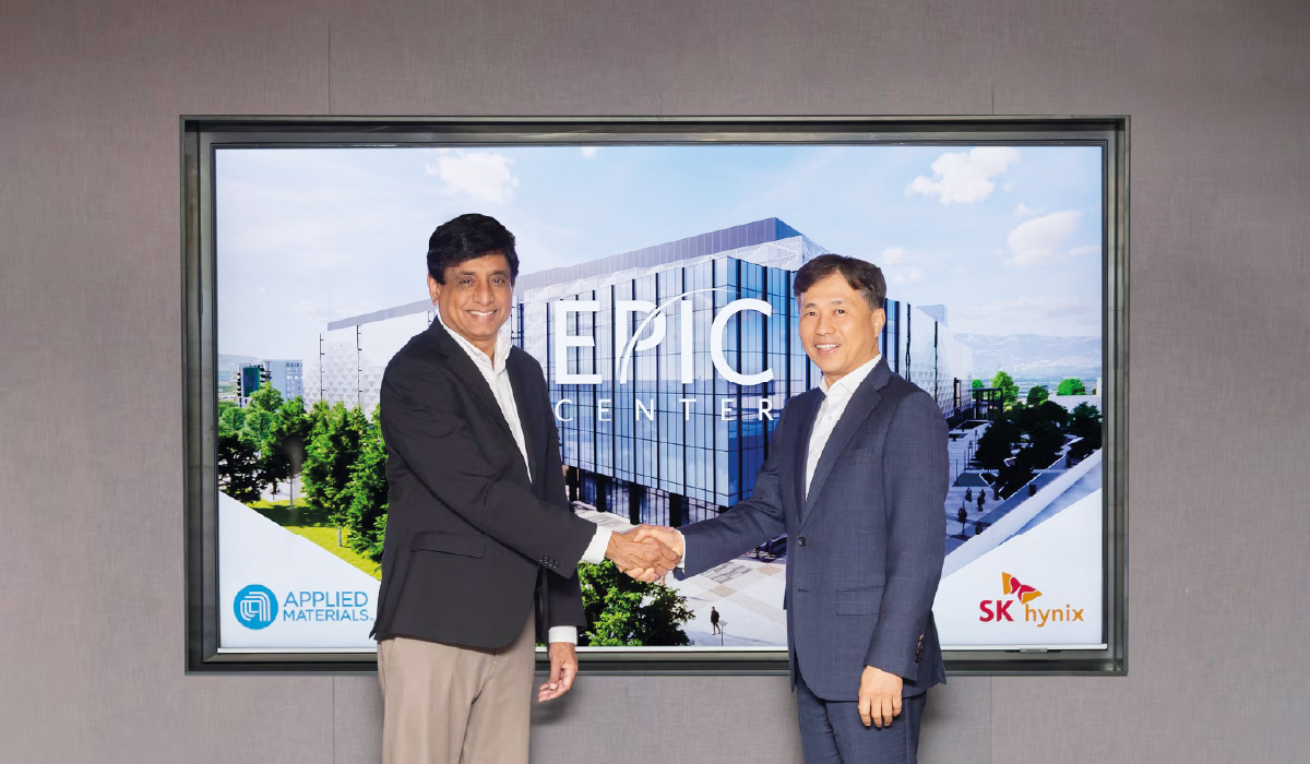
 Prabu Raja, President of Applied Materials’ Semiconductor Products Group and Noh-Jung Kwak, President and CEO of SK hynix
An Innovation Pathway from Research to Mass Production
The significance of this collaboration goes beyond simply expanding the scope of research. By involving technical teams from both companies at the earliest stages of R&D, the partnership will enable them to determine more quickly how new technologies would perform under actual manufacturing conditions and incorporate the findings into subsequent R&D stages. SK hynix will gain early access to technologies under development at Applied Materials and be able to validate them under manufacturing-relevant conditions. Through joint research, Applied Materials will gain a better understanding of technology requirements across multiple process generations, allowing it to refine the direction of its future R&D investments.
When development, validation, and R&D planning are integrated into a single process, the transition to mass production can also be accelerated. As next-generation memory technologies increasingly require devices, processes, and packaging to be considered together, collaboration between manufacturers and semiconductor equipment and materials engineering companies on technology development and validation from the earliest stages of R&D is becoming ever more important.